layer, Technology & APPLICATIONS
Providing next-generation semiconductor material.
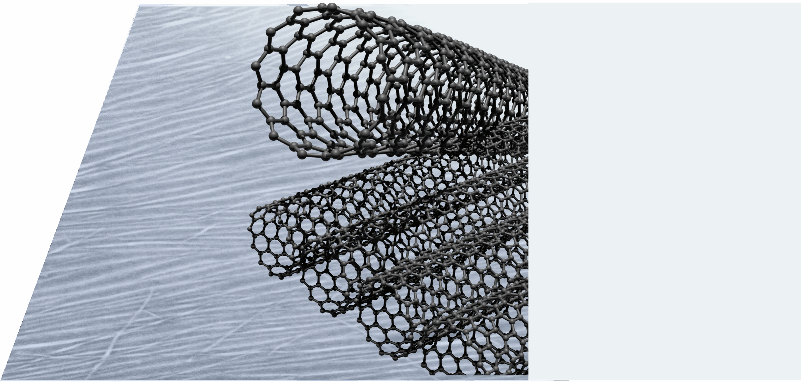
We’ve made it our mission to make high-performance additive semiconductor layers accessible to both research and industry. By enabling FAB-compatible nanomaterial integration at wafer level, we accelerate next-generation sensor innovation and enhance established semiconductor platforms with new capabilities.
Providing next-generation semiconductor material.
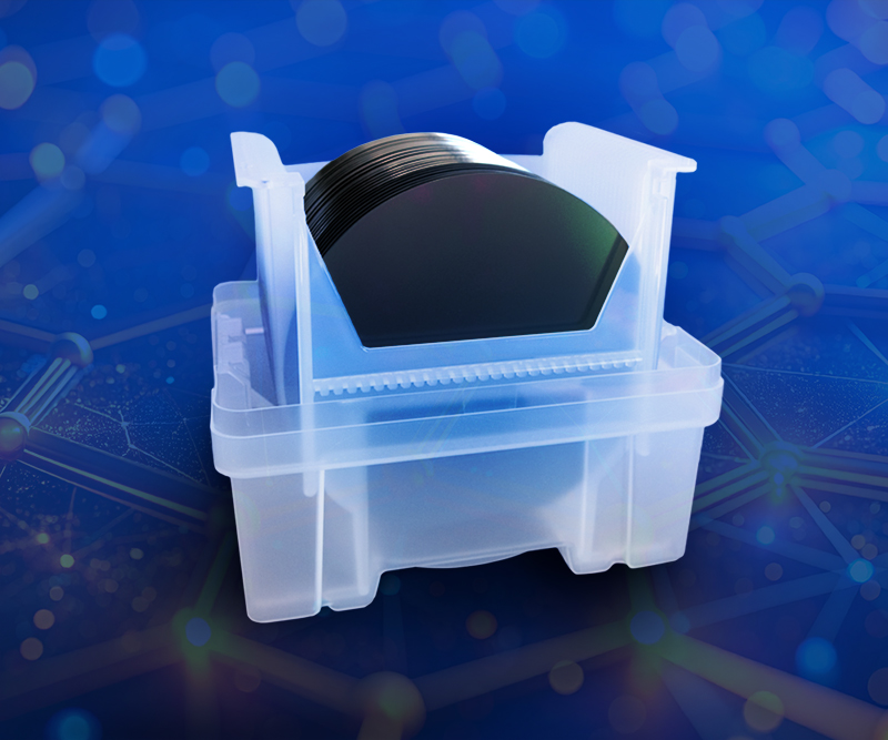
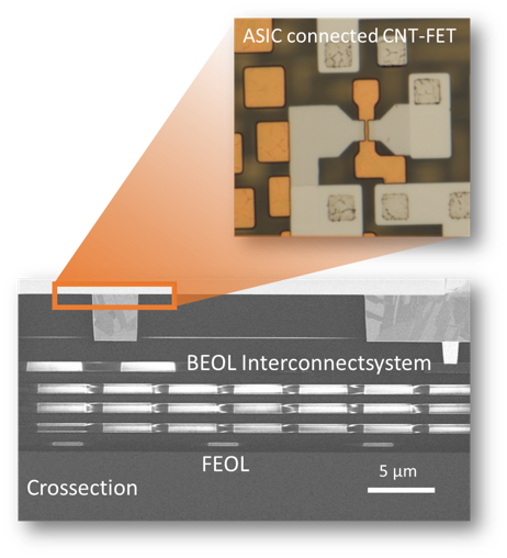
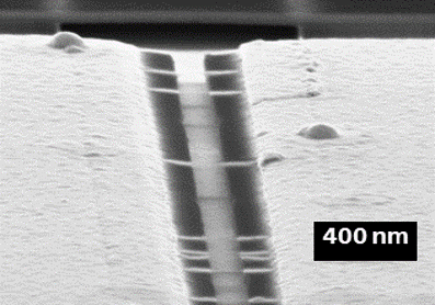
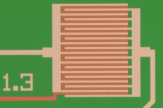
Explore our advanced 200 mm wafer-level CNT layer technology, delivering precisely assembled, homogeneous, and reproducible semiconducting films.
![]()
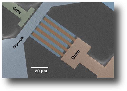
Technology module for field-effect transistors — a versatile foundation for application-specific, high-performance electronics and sensing solutions.

Shape tomorrow — with nanotechnology that redefines integration, functionality, and performance.
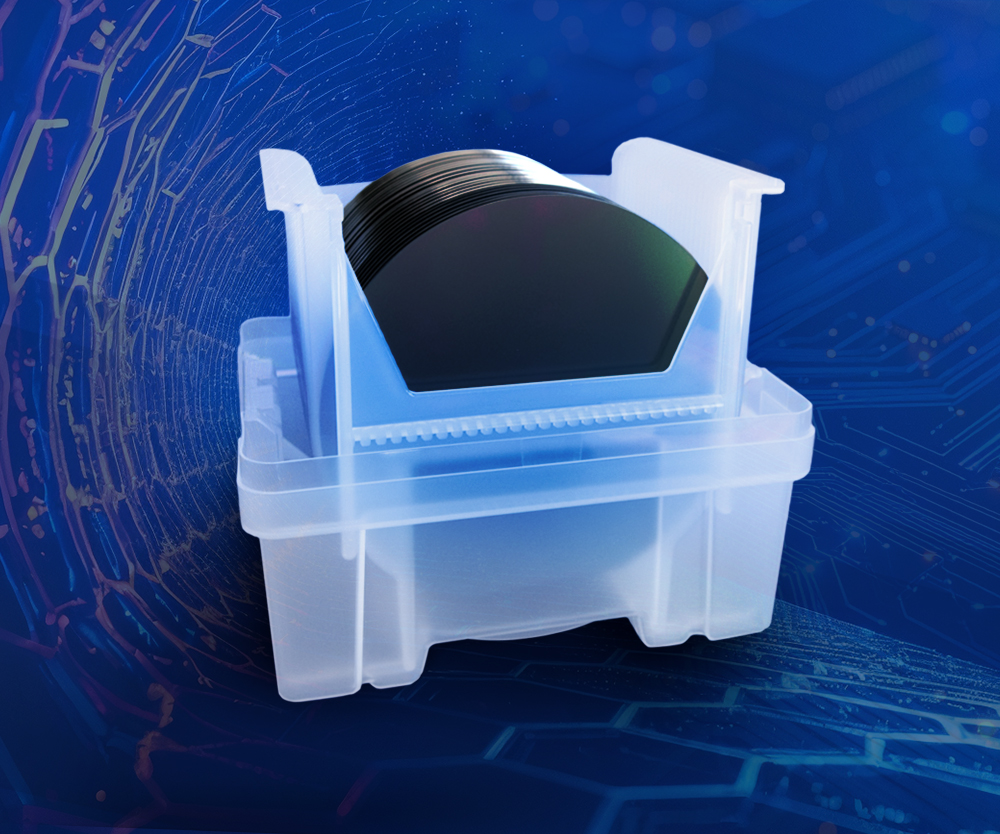
Explore our advanced 200 mm wafer-level CNT layer technology, delivering precisely assembled, homogeneous, and reproducible semiconducting films.
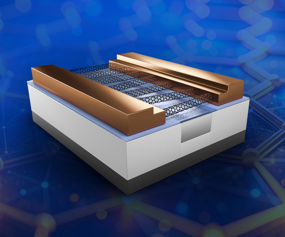
Technology module for field-effect transistors — a versatile foundation for application-specific, high-performance electronics and sensing solutions.
Shape tomorrow — with nanotechnology that redefines integration, functionality, and performance.
Our team combines deep technical expertise and innovative thinking to drive advancements in carbon nanotube technology.

Project lead & Strategy

Technology lead & Development

CNT Integration lead & Research Coordination
Challenge us